-768x679.png "PCB Cross-Section Metrology with Mikrosize iMetal-850-TR Upright Metallographic Microscope 1")
Printed Circuit Boards (PCBs) serve as the core electrical interconnection carrier for modern electronics, integrating conductive traces and insulating substrates. They are universally deployed across consumer electronics, computing hardware, communication equipment, and aerospace-grade electronic assemblies. The popularity of PCBs stems from their merits: high-density circuit layout, outstanding reliability, excellent design flexibility, manufacturability, testability, assembly performance and service maintainability.
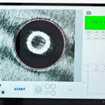
Visual inspection alone cannot verify whether finished PCBs comply with original design specifications. Precision microscopic hardware paired with dedicated metrology software is mandatory for quantitative dimensional verification of PCB cross-section specimens. Many manufacturing sites are required to measure critical cross-section metrics: copper foil thickness, hole-wall copper thickness, solder mask ink thickness, dielectric layer thickness, core substrate thickness, and minimum drilled hole dimension. To address these production-quality demands, Mikrosize delivers a complete inspection solution built around the iMetal-850-TR transflective metallographic microscope, high-resolution microscopic industrial camera and proprietary image-analysis measurement software. This proven turn-key system offers robust performance and streamlined workflows for routine quality-control laboratories.
-300x265.png "PCB Cross-Section Metrology with Mikrosize iMetal-850-TR Upright Metallographic Microscope 2")
Why Choose iMetal-850-TR for PCB Cross-Section Analysis
The iMetal-850-TR transflective upright metallographic microscope features dual illumination (reflected epi-light + transmitted light), delivering large field-of-view, sharp imagery and superior image contrast. It natively supports bright-field and polarizing observation modes, perfectly matching PCB cross-section evaluation requirements.
Built-on an infinite-corrected optical system, the unit incorporates an intelligent light-intensity-management LED system. When users switch objectives, illumination brightness auto-calibrates to optimal levels, eliminating under-exposure artifacts at high magnifications — a common pain point of conventional metallurgical microscopes.
Key hardware specifications relevant to PCB inspection:
- Trinocular observation head: 30° tilt angle; configurable beam-splitting ratios (Eyepiece/Camera: 100/0, 50/50, 0/100), supporting simultaneous visual observation and digital image capture.
- Ultra-wide-field 10 X high-eyepoint eyepieces (field number Φ25 mm) with diopter adjustment, reducing operator visual fatigue during long-duration batch testing.
- M60PLFL series long-working-distance plan semi-apochromatic BD objectives (5 X,10 X,20 X,50 X) deliver exceptional resolution for observing glass-fiber weave texture inside PCB prepreg, copper layers, solder mask and dielectric boundaries.
- 360° rotatable dual-mode polarizer & analyzer (transmission / reflection) enhances contrast for multi-material layered PCB cross-sections.
- Detachable 5-hole encoded motorized nosepiece (M32) with DIC slot records objective metadata into captured image files, cutting human-setup errors in high-volume QC work.
- Dual Köhler illumination architecture:
- Reflected path: Bright-field / Dark-field Köhler LED illumination; 4500 K color temperature, CRI ≥ 95, rated lifespan up to 50 000 hours.
- Transmitted path: Köhler illumination with Abbe condenser (NA = 1.1), compatible with objectives ≥4 X magnification.
- Coaxial coarse-fine focusing system: adjustable friction, 1 μm fine-focus graduation scale plus the prism-assisted focusing (FA) system, enabling stable focusing on uneven PCB cross-section mounts.
- Large-travel double-layer mechanical stage (135 × 125 mm loading area, travel 100 × 100 mm); fitted with light-shield baffle and glass specimen platen for both opaque and translucent samples.
-225x300.jpg "PCB Cross-Section Metrology with Mikrosize iMetal-850-TR Upright Metallographic Microscope 3")
-130x300.jpg "PCB Cross-Section Metrology with Mikrosize iMetal-850-TR Upright Metallographic Microscope 4")
Paired with Mikrosize 20-megapixel microscopic industrial camera via standard C-mount interface (compatible with CCD sensors up to 4/3-inch format), the system transfers high-fidelity imagery to host computers. Operators leverage Mikrosize proprietary microscopic-analysis measurement software (basic measurement package included; advanced analysis module optional) to clearly resolve glass-fiber microstructure and perform precise dimensional gauging of multi-layer PCB cross-section parameters.
Broad Application Scope of iMetal-850-TR Transflective Metallographic Microscope
Thanks to combined epi-reflected and transmitted illumination, the iMetal-850-TR supports observation for both opaque and translucent specimens. Beyond PCB cross-section failure analysis and quality control, this platform is widely adopted across multiple high-tech verticals:
- Semiconductor & FPD manufacturing: inspection of wafer cross-sections and display-panel material characterization.
- Metallic-material metallography: grain-structure observation and material-performance assessment.
- Precision-tool inspection: measuring tool edge profile and surface micro-defects.
- Mineralogy & petrography: polarizing-based identification of mineral thin-section textures.
- Material-science research labs: multi-mode microscopic observation for academic and industrial R&D projects.
-300x235.jpg "PCB Cross-Section Metrology with Mikrosize iMetal-850-TR Upright Metallographic Microscope 5")
-300x225.jpg "PCB Cross-Section Metrology with Mikrosize iMetal-850-TR Upright Metallographic Microscope 6")
-300x230.jpg "PCB Cross-Section Metrology with Mikrosize iMetal-850-TR Upright Metallographic Microscope 7")
Final Summary
For PCB manufacturers, contract-manufacturing houses and quality-control laboratories, accurate cross-section metrology is indispensable to validate circuit-board production quality. The complete Mikrosize iMetal-850-TR inspection ecosystem (transflective metallurgical microscope + high-resolution industrial camera + measurement software) provides reliable, easy-to-deploy hardware-software integration, covering routine incoming inspection, process monitoring and failure-analysis tasks for printed-circuit-board production.
-150x150.jpg)