-1-768x452.png "What Industries Use Metallographic Microscopes? Key Real-World Applications for Material Quality Control 1")
If you are searching for what is an inverted metallographic microscope used for, metallographic microscope industry applications, or how to inspect metal microstructure under microscope, you will find that metallographic microscopes stand out from standard biological microscopes. Unlike biological microscopes designed for transparent biological specimens, a metallographic microscope focuses on examining microstructures, hidden defects and manufacturing quality of opaque materials including metals, alloys, ceramics, semiconductors and composite materials after cutting, grinding, polishing and etching sample preparation.
Manufacturing quality-control labs, failure-analysis teams and material-research institutes heavily rely on this equipment to catch invisible flaws that visual inspection cannot detect. Below we break down its core practical use cases across mainstream industrial verticals.
Automotive Industry: Heat-Treatment Validation for Transmission Gears
One common real-world metallographic microscope application in automotive quality testing is inspection of automotive transmission gears. A gear may look flawless with naked-eye observation. Once sectioned, ground, polished and chemically etched, technicians can observe critical micro-layers under metallographic microscopy: surface carburized layer, martensitic microstructure, core matrix structure, grain boundaries and non-metallic inclusions.
Lab analysts judge whether heat-treatment processes are qualified, verify carburized layer depth meets design specifications, and screen abnormal harmful microstructures. This testing procedure prevents premature gear wear and unexpected transmission failure, which is vital for automotive component reliability validation.
New-Energy Vehicle Sector: Laser-Weld Inspection for EV Battery Connections
For new-energy lithium-ion battery production quality assurance, metallographic cross-section analysis is an indispensable testing workflow. Laser welding between battery tabs and busbars is a key connection process for EV battery packs.
By cutting through welded joints, operators use metallographic microscopes to measure weld penetration depth, weld width and heat-affected zone (HAZ). It also identifies internal hidden defects such as gas pores, micro-cracks and incomplete fusion. These internal defects cannot be spotted by surface visual checks. That explains why metallographic examination of battery laser welds has become a standard quality-control step for new-energy vehicle battery manufacturing lines.
Electronics Industry: PCB and BGA Solder-Joint Cross-Section Analysis
BGA solder joint metallographic inspection for PCB assembly is a well-known workflow within electronics manufacturing. For BGA packaged chips, surface appearance cannot reflect internal solder-joint health status. After metallographic cross-section sample preparation, the microscope visualizes solder morphology, IMC (intermetallic compound) layers, voids, cracks and solder-pad interface conditions.
Matching measurement software can quantify solder-joint dimensions, plating thickness and defect sizes. This workflow supports root-cause failure analysis for short circuits or poor electrical contact on printed circuit boards.
Semiconductor Packaging: Micro-Defect Detection for Chip Encapsulation
In semiconductor packaging failure analysis labs, metallographic microscopes inspect cross-sectioned packaging assemblies. Operators observe layered structures including silicon die, solder layers, copper traces, lead frames and epoxy molding compounds.
Primary inspection targets cover interface delamination, micro-cracks, void formation, bonding integrity and metallic layer thickness. These observations help engineers optimize packaging processes and improve long-term chip operational stability.
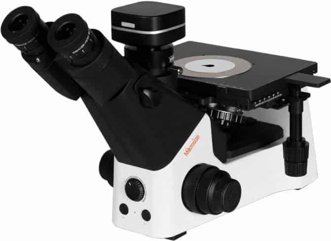
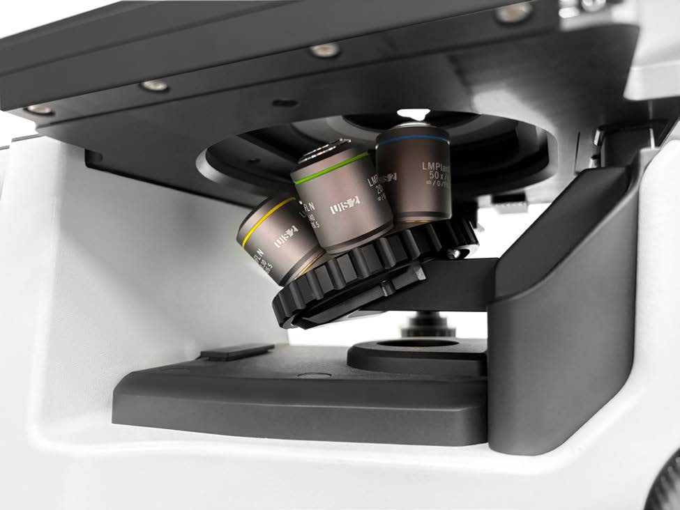
Advanced Instrument for Multi-Industry Metallographic Testing: Mikrosize iMetal-300 Inverted Metallographic Microscope
To satisfy high-precision testing requirements across automotive, new-energy battery, electronics and semiconductor sectors, the iMetal-300 Inverted Metallographic Microscope developed by Mikrosize delivers reliable optical performance and user-friendly automation featuresMikrosize.
- It adopts an infinite optical system, paired with plan semi-apochromatic objective lenses and wide-field high-eyepoint eyepieces, faithfully restoring fine metallographic microstructure details for high-precision detection requirements.
- Full-series objectives support long working distance performance. Even at maximum 50× magnification, it retains an 8.5 mm working distance. Users can observe large-size and special-shaped specimens without frequent re-preparation, greatly boosting lab detection efficiency.
- When switching objective magnifications, the unit automatically sets optimal light intensity. It removes repetitive manual adjustment steps, cuts human-induced errors and delivers smooth continuous inspection workflows.
- Equipped with a 4000K-4300K warm-white LED light source with CRI ≥95, it reproduces authentic sample colors. It avoids misinterpretation triggered by color distortion and fits metallographic rating and quantitative image-analysis tasks.
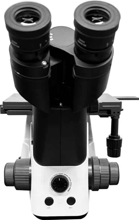
- The 45° inclined hinged trinocular tube with a 100:0/0:100 beam-splitter ratio supports simultaneous human-eye viewing and imaging-system connection. It fulfills photo capture, video recording and digital-archive demands for lab test reports.
- A coaxial coarse-fine focusing system with 1 μm fine-focus graduation, a 50 × 50 mm large-travel stage and a 5-hole coded nosepiece guarantee precise positioning, smooth operation and sustained measuring accuracy over long-term heavy-duty laboratory usage.
Whether you run routine production quality screening or complex failure-analysis projects, the Mikrosize iMetal-300 fits diversified metallographic testing scenarios across multiple industries.
Conclusion
Metallographic microscopes serve as foundational material-characterization instruments for automotive component verification, new-energy battery weld quality control, PCB solder-joint evaluation and semiconductor packaging inspection. They expose invisible micro-level defects that ordinary visual inspection cannot capture, supporting manufacturers to optimize processes, cut failure risks and maintain product reliability.
When labs are looking for high-performance inverted metallographic microscopes for multi-industry material testing, Mikrosize offers the iMetal-300 Inverted Metallographic Microscope as a practical solution. Its infinite optical architecture, long-working-distance objectives, smart illumination adjustment and high-CRI lighting address real-world pain points for metallographic technicians, covering sample observation, image capturing and quantitative metallographic rating workflows for modern industrial quality-control laboratories.
-150x150.jpg)